
With LoRa devices (long range), it is easy to create a low-power wireless device for IoT networks that uses a very low level of power. Since Lora technology is one of the best IoT technology communication, in that regard, all considerations for IoT design are used for Lora wireless PCB design. Since the design ecosystem in IoT PCB design is different from typical electronics products, we need to take a different approach.
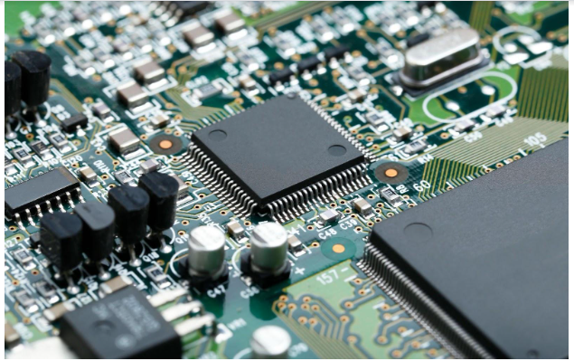
IoT devices such as smart wearables need smaller-sized electronic components and limited PCB routing areas, due to the limited size. It makes multilayer PCBs a necessity. While designing a Lora wireless design board, PCBs with flex structure have a mechanical structure that affects component placement, so we sometimes need to use flex PCBs instead of rigid PCBs. Also, Batteries that power IoT devices require proper power management to extend their lifespan.
The design will need to remain within its power budget not only by choosing the right power management ICs but also by selecting the right blocks within the design.
So, the purpose of this article is to highlight PCB design requirements that should be included in Lora wireless design boards.
Lora Module
Microprocessors and radio modules are the main components of LoRa modules, which are commonly referred to as end nodes or end devices. In most cases, the end node is powered by a battery, but it can also be powered by main electricity. Radio module modulators encode data into carrier signals so they can send signals to gateways.
In addition to various types of modulation, LoRa also uses spread spectrum modulation as a signal modulation technique. Space and military communication have been using this technique for decades due to its low susceptibility and long-range communication capacity for the interface.
Also, for wireless applications, it is vital to implement lightweight planar antenna structures on a common PCB platform where the processing and microcontroller unit is connected. It is also often performed with a push-on miniaturized coaxial interface. A LoRa network allows transferring of small amounts of data off-grid, which makes it a fantastic IoT technology. So, LoRa transceivers and GPS modules can be combined to create a device that can be used for a variety of sensing applications.
In addition to this, for LoRa wireless PCB board design, the design and placement of the antenna can have a significant impact on link integrity. Environmental interference, metallic enclosure hardware, and neighboring electronic components can all impact radiation quality directly. Also, to expand the link budget, there is a need to consider several factors, such as transmit antenna gains, miscellaneous environmental losses, free space path loss, antenna feed loss, and transmitter and receiver losses.
A LoRa wireless PCB board connection’s first steps include evaluating parameters such as radiation pattern, gain, VSWR, and bandwidth regardless of the environment.
Lora Wireless Board Design
Lora’s wireless PCB board design is critically dependent on the integrity of the wireless link between nodes, link budget, and antenna. Some of the most popular antennas are PCB antennas, rubber duck antennas, sucker cap magnetic mount antennas, spring antennas, fiberglass antennas, and FPC antennas.
So, as per the frequency and power of the LoRa module, LoRaWAN node, and LoRa gateway, you can select any of the above-mentioned antennas. However, it would be best to use PCB antennas as they can be multi-pole, slot, printed inverted-F (PIFA), patch, and dipole. IoT sensor technologies, protocols, and vendor-specific SoCs often overlook the antenna, link budget, and integrity of the wireless connection between nodes.
Nevertheless, it is usually possible to communicate with IoT devices using a PCB antenna or chip antenna that has an omnidirectional radiation pattern with a vertical or horizontal beamwidth. Also, if you need to extend the range, you can use directional antennas (Yagi) when you need to connect specific fringe devices.
There are benefits and considerations associated with each antenna type. PCB antennas have a low profile, so they can be easily configured within cases instead of sticking out like whip antennas. A PCB antenna, on the other hand, can operate over a wider bandwidth and achieve a higher gain than a chip antenna. So, when we talk about PCB design considerations for LoRa wireless board design, PCB antennas are both efficient and compact and extremely effective in this case.
Considering EMI Standards on Lora PCB Design
Every electronic device needs EMI to function properly. In other words, it is a measure of how resistant an electronic device is to external noise to operate efficiently. Also, the best EMI-performance PCB has three main characteristics, including the following.
- Having immunity against the emission EM of other PCBs
- It doesn’t interfere with other PCB boards, and
- Doesn’t intrude on its operation
In addition, electronic devices without EMI compliance, even if they have the best functionality, are not marketable. Therefore, all requirements and standards about electronic systems must be met, in addition to their quality standards.
Also, the EMI comes from an external layout, PCB layout, and electronic components. So, with high voltage consumption, electronic components prepare EMI. Some of the main factors that cause EM emission from the PCB layout include poor capacitance coupling, high-frequency traces, impedance mismatching, and switching circuits. In that regard, the following are some suitable design practices to reduce EMI.
- Use low-power electronic components when using components with high power consumption to reduce EM emissions.
- Using SMDs (surface mount devices) in high-frequency applications reduces RF emissions and provides lower resistance and inductance.
Moreover, using a Faraday cage for sensitive electronic components also prevents RF emissions into the environment and protects them from external EMI.
Conclusion
To sum up, there are several things to consider when designing a LoRa wireless PCB board and comparing its sensitivity or performance. Also, it is significant to analyze the design to provide a proper and effective comparison. The PCB design, even the choice of passive components, has a significantly greater impact on sensitivity than the concentrator. And Arshon technology can design and manufacture PCBs for any application, including PCBs for LoRa products.
Author: Sherry Mosleh IoT Development Engineer at Arshon Technology Inc.